Blog on RFID Technology and IoT Solutions
Blog Home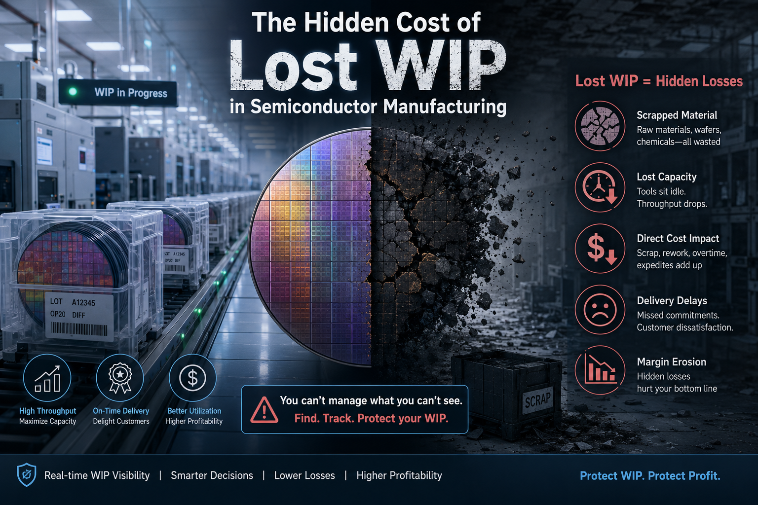
The Hidden Cost of Lost WIP in Semiconductor Manufacturing
25 June 2026Semiconductor fabs are among the most capital-intensive facilities ever built, with new plants costing anywhere from $17 billion to $100 billion. Yet beneath the polished cleanrooms and billion-dollar lithography tools sits a quieter, almost invisible drain on profitability: lost Work-in-Progress, or “lost WIP.”
What Lost WIP Actually Means
“Lost” WIP happens when wafer lots are delayed, misrouted, or simply stuck in the line because of poor floor visibility or unplanned equipment downtime. Manufacturing economics has a simple rule for this: WIP equals throughput multiplied by cycle time. The moment a lot stalls, cycle time inflates, and capital that’s already sunk into wafers, rare chemicals, and energy sits frozen on the floor, generating zero return while the clock keeps running.
The Real Price Tag
The numbers get uncomfortable fast. A yield slip of just half a percentage point, often traceable to mishandled or bottlenecked WIP, can cost a major fab tens of millions of dollars a year. Unplanned downtime tied to WIP congestion can drain millions of dollars per hour in lost production. And the cost of a defect is anything but linear, a flaw caught at wafer scrap is cheap to absorb, but the same flaw discovered after system-level test, or worse, after it reaches a customer as a field failure, can cost dramatically more once recalls, charge-backs, and SLA penalties enter the picture.
- 0.5%yield drop can cost a fab tens of millions annually
- 10–100xcost escalation from wafer scrap to field failure
- $M/hrlost to unplanned downtime on a congested line
The pain compounds in Asia-Pacific, which holds over half of the global semiconductor market. Advanced-node production at 2nm and 3nm requires hundreds of routing steps, multiplying the odds of misrouted lots. Multi-country supply chains mean a single fab’s delay ripples straight through downstream assembly and test partners, and a widening talent gap is stretching manual tracking systems past their limits.
Why Spreadsheets Can’t Catch It
The traditional yield-quality-cost triangle that manufacturing has relied on for decades is buckling under sub-2nm nodes and heterogeneous integration. Testing and quality assurance alone can now consume up to 30% of total manufacturing cost. Throwing more inspection at the problem doesn’t fix it, because the root issue isn’t testing, it’s visibility. You can’t manage what you can’t see, and manual, spreadsheet-driven lot tracking simply wasn’t built for fabs running this much complexity at this much speed.
Cost-cutting through corner-cutting only accelerates field failures down the line. The fix isn’t less inspection, it’s real-time visibility.
Turning a Hidden Cost Into a Competitive Edge
This is precisely the gap IntelliStride was built to close. As an RFID and IoT solutions provider with deep manufacturing experience across Asia-Pacific, IntelliStride attacks lost WIP at its source: visibility.
By embedding RFID tags directly into Front-Opening Unified Pods, the carriers that move wafers through the line, IntelliStride gives fabs automatic, real-time identification of every lot’s location. That single change replaces manual scanning and guesswork with continuous, accurate tracking, directly targeting the “delayed or misrouted” problem at the heart of lost WIP. The same RFID backbone extends to high-value tools, spare parts, and consumables, so nothing critical goes missing when a line is running at full tilt.
On the equipment side, IoT sensors continuously monitor temperature, vibration, and power consumption, feeding data into IntelliStride’s CrossTalk platform to enable predictive maintenance before a tool fails and stalls the floor. Combining that sensor data with RFID location data gives operations teams a genuinely holistic view of equipment health and utilization, all integrated with existing backend MES and IT systems rather than bolted on as another disconnected dashboard.
The Bottom Line
The fractured yield-quality-cost triangle isn’t getting simpler, and cost-cutting through corner-cutting only accelerates field failures down the line. The fabs that win the next decade will be the ones that trade reactive blindness for real-time visibility. Turning the hidden cost of lost WIP into a competitive advantage starts with seeing your floor clearly, and that’s exactly where IntelliStride’s RFID and IoT solutions come in.
See where your WIP is actually going
IntelliStride helps semiconductor manufacturers replace manual lot tracking with real-time RFID and IoT visibility, from FOUPs on the line to predictive maintenance on the tools that move them.
- Intellistride.com
- Blog
- The Hidden Cost of Lost WIP in Semiconductor Manufacturing